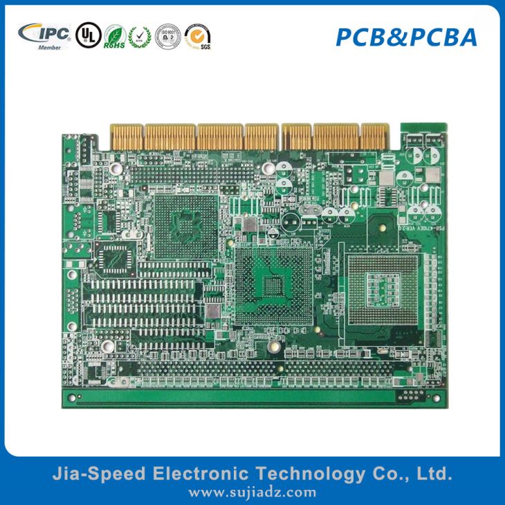


HDI PCB (High Density Interconnect)
-
Payment


-
Origin
China Mainland
-
Minimum Order
5
-
Packing
Pieces
- Contact Now Start Order
- Description
Product Detail
Blind and/or buried vias
Via-in-pad
Through vias from surface to surface
20 µm circuit geometries
30 µm dielectric layers
50 µm laser vias
125 µm bump pitch processing
HDI PCB (High Density Interconnect)
HDI is an abbreviation of High Density Interconnector. It is a kind of technology (technical) for producing printed boards, and a circuit board with a relatively high density of wiring distribution using the micro blind buried hole technology. HDI is a compact product designed for small capacity users. It adopts a modular and parallel design, a module capacity of 1000VA (1U in height), natural cooling, can be directly placed into a 19” rack, and can be connected in parallel to a maximum of 6 modules. This product uses all-digital signal process control (DSP) technology and many The patented technology has a full range of adaptability to load and a strong short-term overload capability, regardless of load power factor and crest factor.
HDI circuit advantages
1 Reduces PCB cost: When the density of the PCB increases more than eight layers, manufacturing with HDI will cost less than the traditional 2 complex lamination process.
3 Increase the line density: the interconnection of traditional circuit boards and parts
4 conducive to the use of advanced packaging technology 
5 has better electrical performance and signal correctness
6 Better reliability
7 can improve thermal properties
8 Improves RF/Electromagnetic/Electrostatic Discharge (RFI/EMI/ESD)
9 Increase design efficiency [1]
The HDI PCBs we offer include the following highly requested characteristics:
Our high density circuit boards have the technology-pushing capabilities to drive applications in a large number of industries including but not limited to semiconductor test equipment, defense, medical and aerospace.
JIA-Speed can provide you with the highest quality HDI PCB, please do not hesitate to contact us TEL: +8613186089157
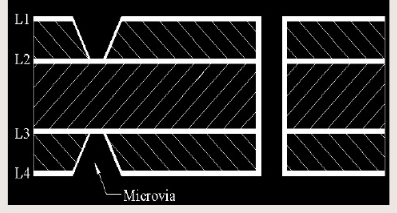
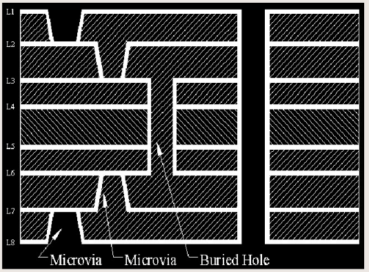
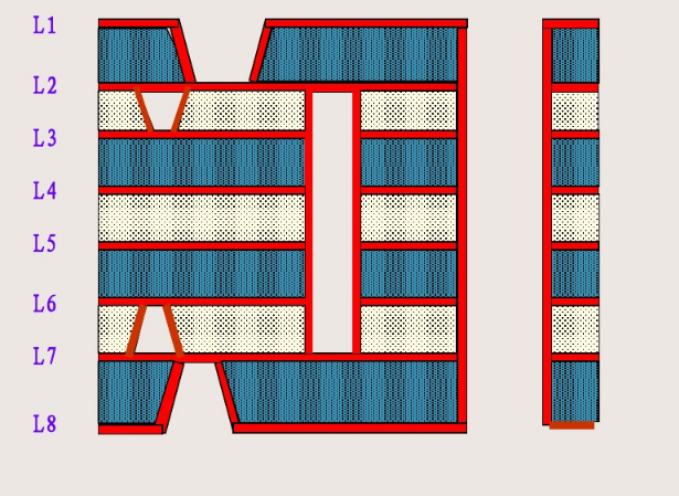
HDI PCB board stack structure
Blind hole, through hole, without buried hole
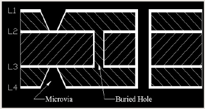
With Blind hole, through hole and buried hole
6-layer HDI PCB (1+4+1 layer)

Blind hole, through hole, without buried hole
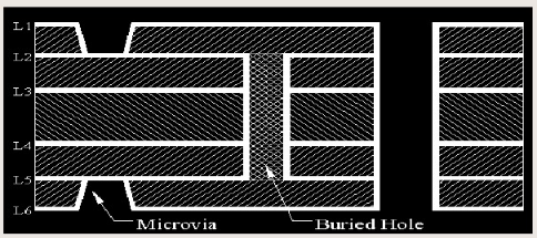
With Blind hole, through hole and buried hole
8-layer HDI PCB (1+4+1 layer)
Blind hole, through hole, without buried hole
With Blind hole, through hole and buried hole
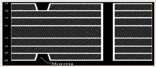
HDI PCB second-order blind hole
HDI PCB second-order blind hole: the blind hole that leads from the outer layer to the third layer can be directly turned on 1-3 layers, and can also be turned on 1-2 layers, 2-3 layers( 1+1+4+1+1 layer)
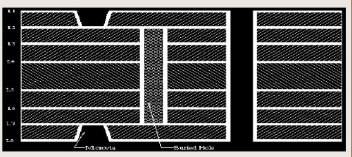
HDI PCB Second Order Blind Hole (1+6+1 layer)
HDI PCB capabilities
| Feature | Capability |
| Quality Grade | Standard IPC 2 |
| Layers | 4 - 24layers |
| Build Time | 2days - 5weeks |
| Material | FR4 standard Tg 140°C,FR4 High Tg 170°C, FR4 and Rogers combined lamination |
| Board Size | Min 6*6mm | Max 457*610mm |
| Board Thickness | 0.4mm - 3.0mm |
| Copper Weight (Finished) | 0.5oz - 2.0oz |
| Min Tracing/Spacing | 2.5mil/2.5mil |
| Solder Mask Sides | As per the file |
| Solder Mask Color | Green, White, Blue, Black, Red, Yellow |
| Silkscreen Sides | As per the file |
| Silkscreen Color | White, Black, Yellow |
| Surface Finish | HASL - Hot Air Solder Leveling Lead Free HASL - RoHS ENIG - Electroless Nickle/Immersion Gold - RoHS Immersion Silver - RoHS Immersion Tin - RoHS OSP - Organic Solderability Preservatives - RoHS |
| Min Annular Ring | 4mil, 3mil - laser drill |
| Min Drilling Hole Diameter | 6mil, 4mil - laser drill |
| Max Exponents of Blind/Buried Vias | stacked vias for 3 layers interconnected, staggered vias for 4 layers interconnected |
| Other Techniques | Flex-rigid combination Via In Pad Buried Capacitor (only for Prototype PCB total area =1m²) |
Xi'an JIA-SPEED Electronic Technology Co., Ltd. can provide you with customized HDI PCB according to your requirements. Please send your PCB geber file to emal : jiaspeed243@yahoo.com, or directly call USD : +8613186089157, us Will provide you with detailed quote within 2 hours
-
SMT Through Hole Electronic PCB Circuit Board Assembly 5 Pieces / (Min. Order)
-
Automated Optical Inspection 5 Pieces / (Min. Order)
-
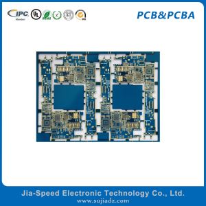
Immersion Gold Pcb Multilayer Circuit Board With Blue Solder Mask 5 Pieces / (Min. Order)
-
Immersion Gold Pcb Multilayer Circuit Board With Blue Solder Mask 5 Pieces / (Min. Order)
-
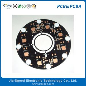
Black Solder Mask Round LED PCB Board 5 Pieces / (Min. Order)
-
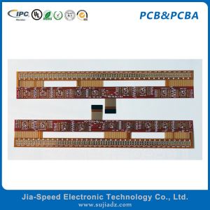
4 layer Flexible PCB / FPC Assembly 5 Pieces / (Min. Order)
 Favorites

-
SMT Through Hole Electronic PCB Circuit Board Assembly
5 Pieces / (Min. Order)
-
Automated Optical Inspection
5 Pieces / (Min. Order)
-
Immersion Gold Pcb Multilayer Circuit Board With Blue Solder Mask
5 Pieces / (Min. Order)
-
Immersion Gold Pcb Multilayer Circuit Board With Blue Solder Mask
5 Pieces / (Min. Order)
-
Black Solder Mask Round LED PCB Board
5 Pieces / (Min. Order)
-
4 layer Flexible PCB / FPC Assembly
5 Pieces / (Min. Order)